How to Design Pcb Layout Using Multisim
It's a great time to be an electronics engineer and an even better time to be a weekend warrior tinkerer. The line between these two worlds is rapidly evaporating as the tools that enable circuit design plummet in cost and skyrocket in capability. The most important thing that a product can do for us is to streamline our workflow while still delivering high quality results.
MultiSIM BLUE, a project spearheaded by Mouser and NI, is one such product. If you haven't done so already, head over to the MultiSIM BLUE website and download the software. It's free. That's a hard price to beat especially for makers who would much rather spend money on project materials. If you are just getting started but are looking to do a little more than just blink and LED, here are some key benefits that might just entice you to give the software a try:
1. SPICE Simulation: There are quite a few decent circuit capture and PCB layout tools, but reliable simulation packages are hard to find. MultiSim Blue supports simulation with the Berkeley Spice engine.
2. Board Size and Layers: Again, most decent tools limit you to ridiculously small footprints or to two signal layers unless you are willing to spend a significant amount of money. MultiSim Blue is very useful when you are looking to creating more complex boards that you intend to have manufactured.
3. Integrated BOM Ordering: Yes I know, I should probably check part availability before I do a PCB design. Even if I do, it's a tedious process. MultiSIM BLUE ties nicely into Mouser's extensive part catalog so you know how many you can buy and what it's going to cost.
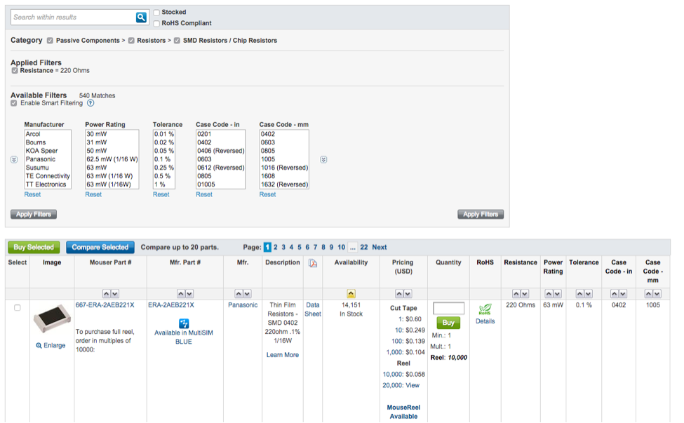
Figure 1A: Always check to see if a component is available in MultiSIM BLUE
4. Footprints: Nothing is worse than selecting a component only to discover that the component is not available in my CAD tool library. Now when I search Mouser for components I always look for the "Available in MultiSIM BLUE" icon.
5. User P/N Labeling: A small but nice feature. You can have your own part numbers printed on the packaging that Mouser ships you. Simply ensure that the "User P/N" field is completed in your BOM. When your components arrive, you'll smile knowing how easy it is to associate a component with its place on your PCB.
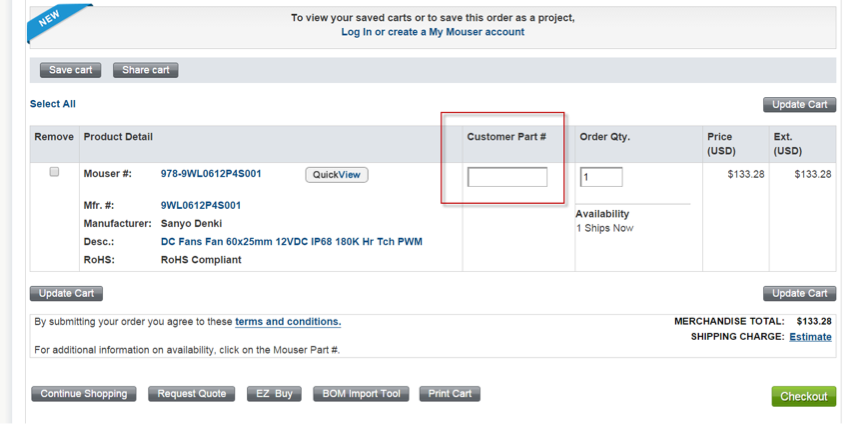
Figure 1B: Shows a cart. If you put a part number in the Customer Part # box, Mouser Electronics will ship that part with a label that matches. This is a nice feature to quickly sort out parts for schematics.
6. 3D Board Viewer: Another feature that tends to cost extra in many design tools is part of the package. Once you have laid out your PCB you can, with a single click of the mouse, view an interactive 3D model of the board. Also, it makes nice eye candy for your website if you are trying to promote your project.
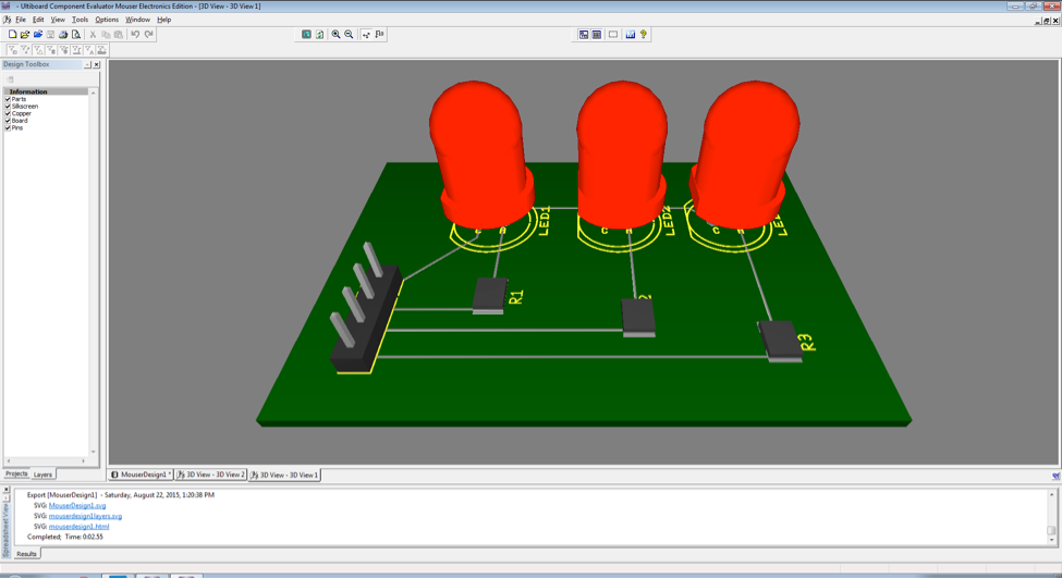
Figure 2: 3D Models help to visualize that the final board will look like, useful when building enclosures or mechanical parts of a project.
No matter what, learning CAD tools is an invaluable and easily transferable skill that I encourage anyone who is dabbling in electronics to learn. If for nothing else, it makes documenting circuit designs so much easier to read as compared to most hand drawn designs. Again, it's hard to argue with free when talking about the value gained from MultiSIM BLUE, especially considering the ability to play with simulated circuits before you build it with real components.
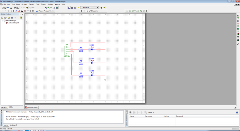
Figure 3: Initial circuit capture in a schematic format.
The most important feature for a homebrew warrior is going to be the ability to do a PCB layout and turn it into an actual circuit board at home. Thankfully, included in the MultiSIM BLUE download is a tool called Ultiboard that lets you do PCB layouts. The goal of using Ultiboard is to get an exportable image file (e.g. PNG or JPG) that we can use to etch a circuit board using a few chemicals and some common household items.
Ultiboard is a pretty straightforward PCB layout tool with just a few things to remember:
1. All components are imported to Ultiboard in a less ideal orientation. Take the time to lace components smartly and use the Design Rule Checker (DRC checks physical layout) and Electrical Rule Checker (ERC checks signal logic) often to ensure your layout is sound.
2. Use the "Follow Me" tool to route your traces. First make sure you are on the top copper layer and then select a component pad. Next use the shortcut 'Ctrl-T' to begin routing. Ultiboard will give you some guidance on where to route but ultimately the choice is yours. I run the DRC and ERC after every trace just to be safe.
3. Once you have all traces routed and no DRC or ERC errors, it's time to create an image file that we can use for the homebrewed etching process. Since we are creating a single trace layer using the top copper layer, we will uncheck all other layers. Lastly, access the Export SVG option from File > Export to create a .SVG image file that we can print on glossy paper on a LaserJet printer which we can transfer to our copper clad boards. This is known as the "toner transfer" method.
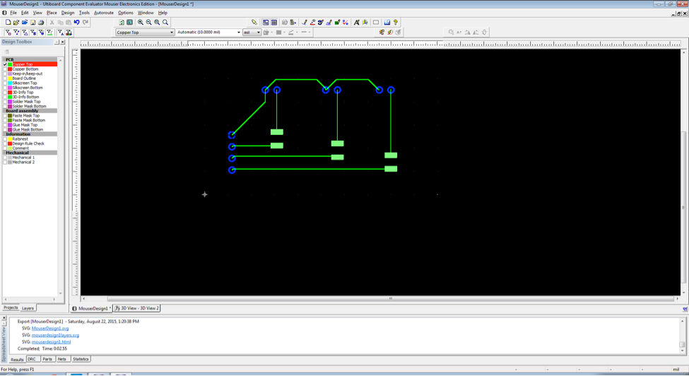
Figure 4: PCB layout with only the necessary layers shown in order to etch or mill a PCB
Before we wrap this blog up, here are some other rules of thumb I use in my designs when I am looking to do a homebrewed PCB:
1. When it comes to components, you might want to start with through-hole components first. When you are ready to try surface mount, I recommend trying 2010 (5025), 1210 (3225 metric), 1206, or 0805 footprints for resistors or capacitors. When it comes to integrated circuits I look for SOT89, SOT223, DPAK, D2PAK, or SOIC footprints.
2. Try to keep designs simple and limit yourself to a single trace layer if possible. Double layer is possible but you will have to hand drill and solder the vias.
3. Speaking of drill bits, I like to stock up on 0.7mm and 0.9mm spiral flute tungsten carbide micro drill bits that I can use in a Dremel rotary tool drill press. Bits will break and there is nothing worse than having to wait for new bits to be delivered.
Have you used MultiSIM BLUE to create homebrewed circuit boards? Let us know in the comments below.
« Back
 Michael Parks, P.E. is the owner of Green Shoe Garage, a custom electronics design studio and technology consultancy located in Southern Maryland. He produces the S.T.E.A.M. Power podcast to help raise public awareness of technical and scientific matters. Michael is also a licensed Professional Engineer in the state of Maryland and holds a Master's degree in systems engineering from Johns Hopkins University.
How to Design Pcb Layout Using Multisim
Source: https://www.mouser.mx/blog/blogpage/45/postid/0/blog/multisim-blue-and-the-homebrewed-circuit-board
0 Response to "How to Design Pcb Layout Using Multisim"
Post a Comment